Analog Accessory Module Design & Development


Industrial Project
Rinstrum (Pvt) Ltd
Principal Supervisors
- Eng. Dane Allison
Group Members
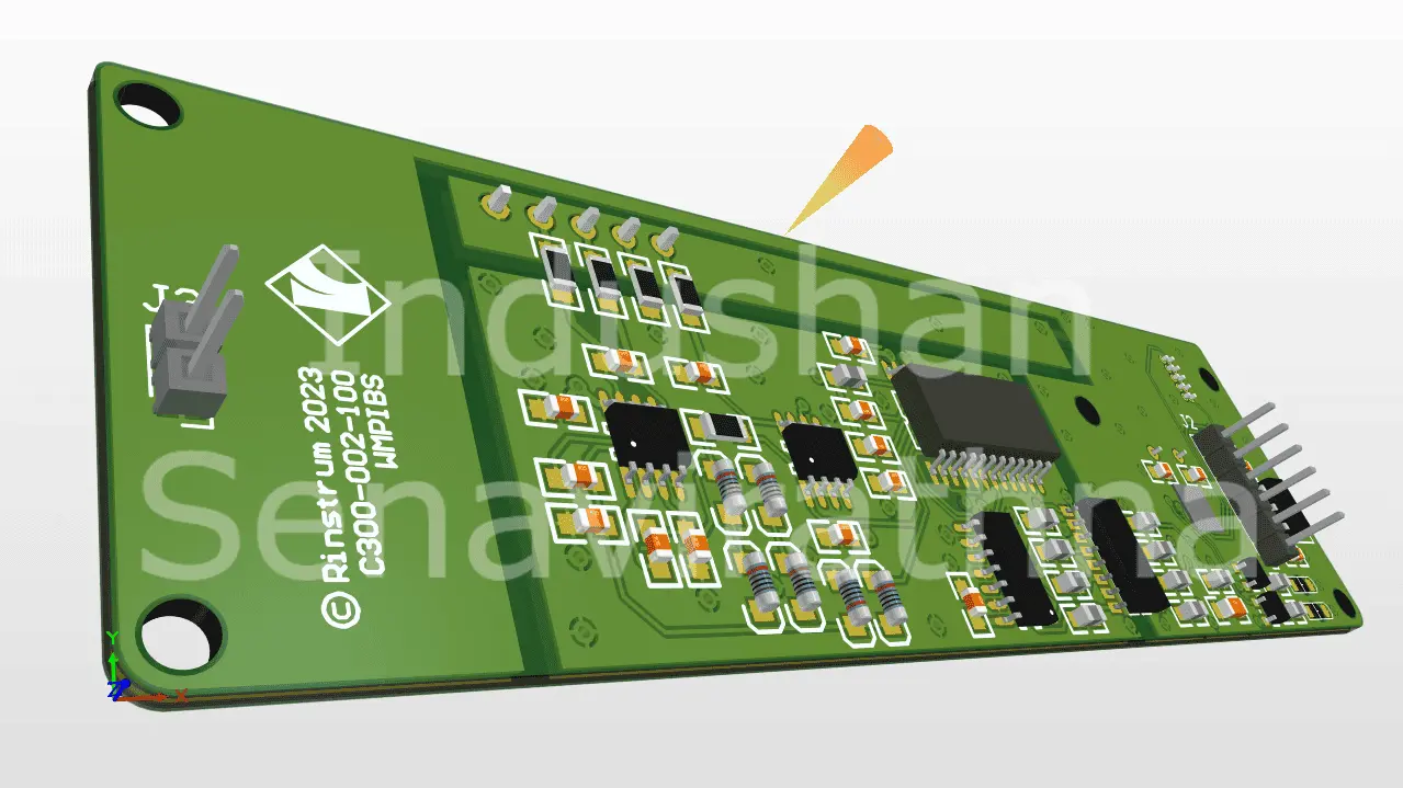
I have successfully completed a professional project as a Design Engineer at Rinstrum (Pvt) Ltd. The project involved the development of an Analog Accessory Module, which provides enhanced analog functionality for industrial applications. The module is designed to deliver a single isolated analog output with a range of either 4-20mA or 0-10V. It achieves a remarkable update rate of up to 400Hz with exceptional resolution of 1/65,000 (16-bit).
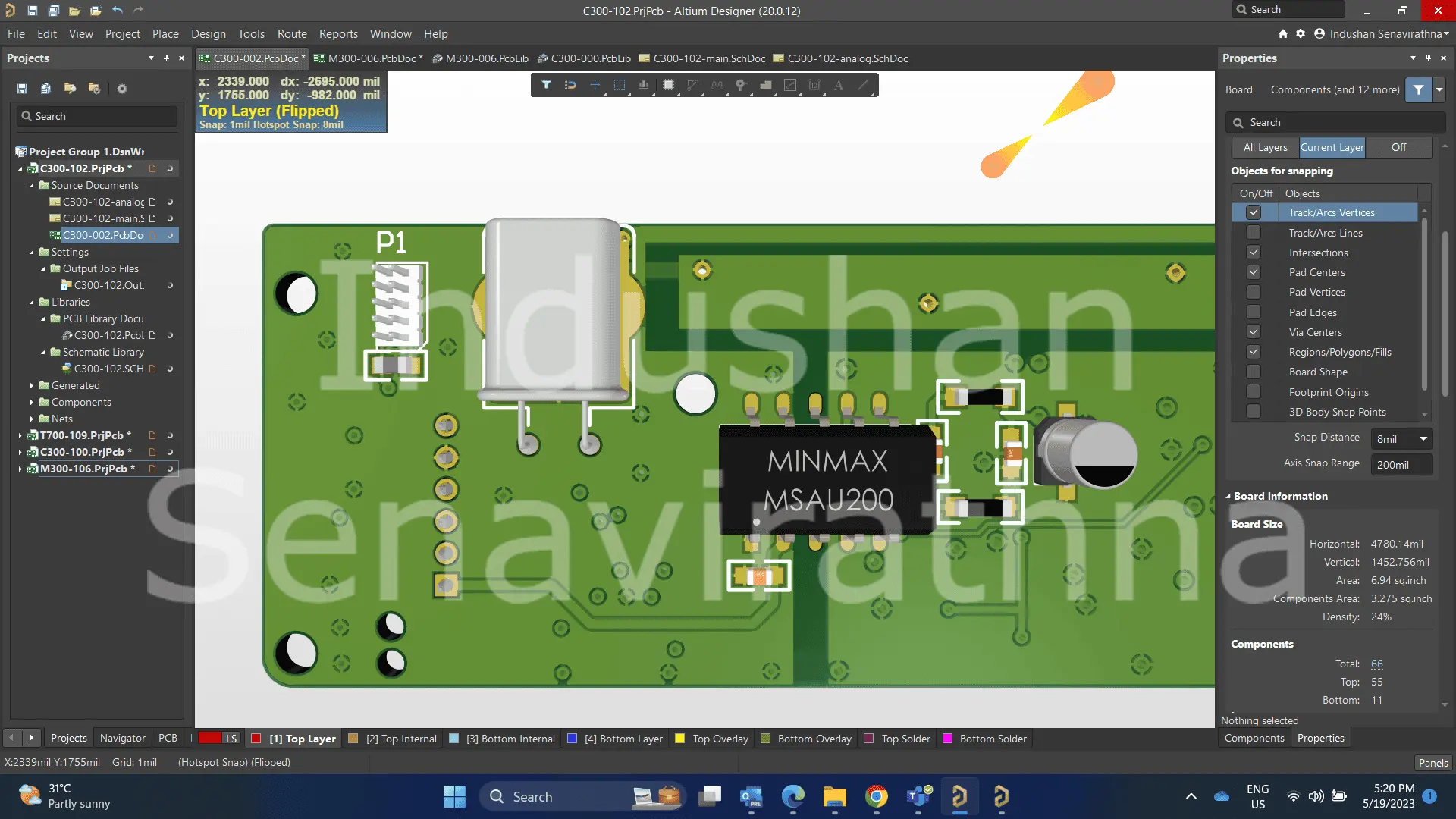
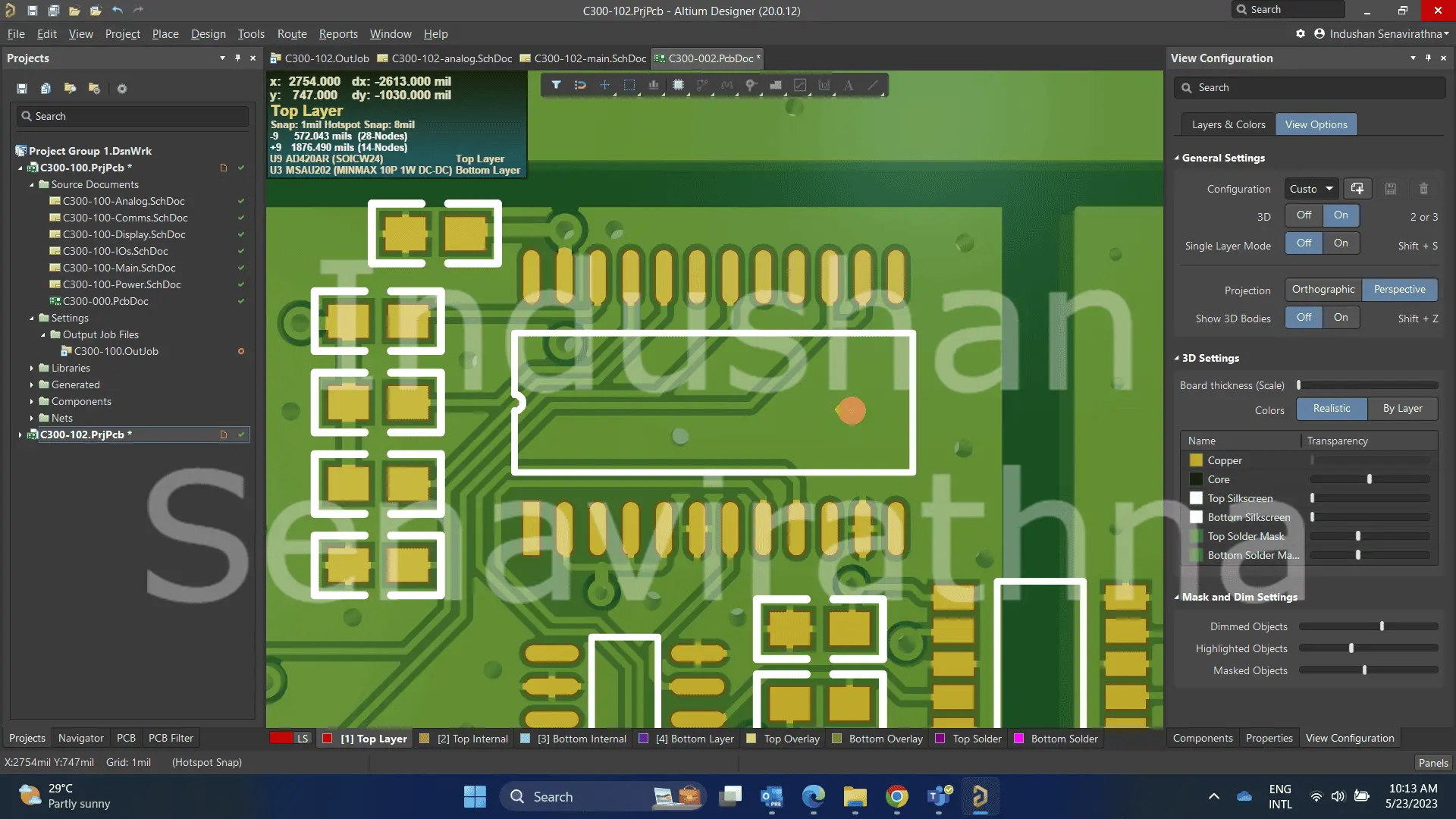
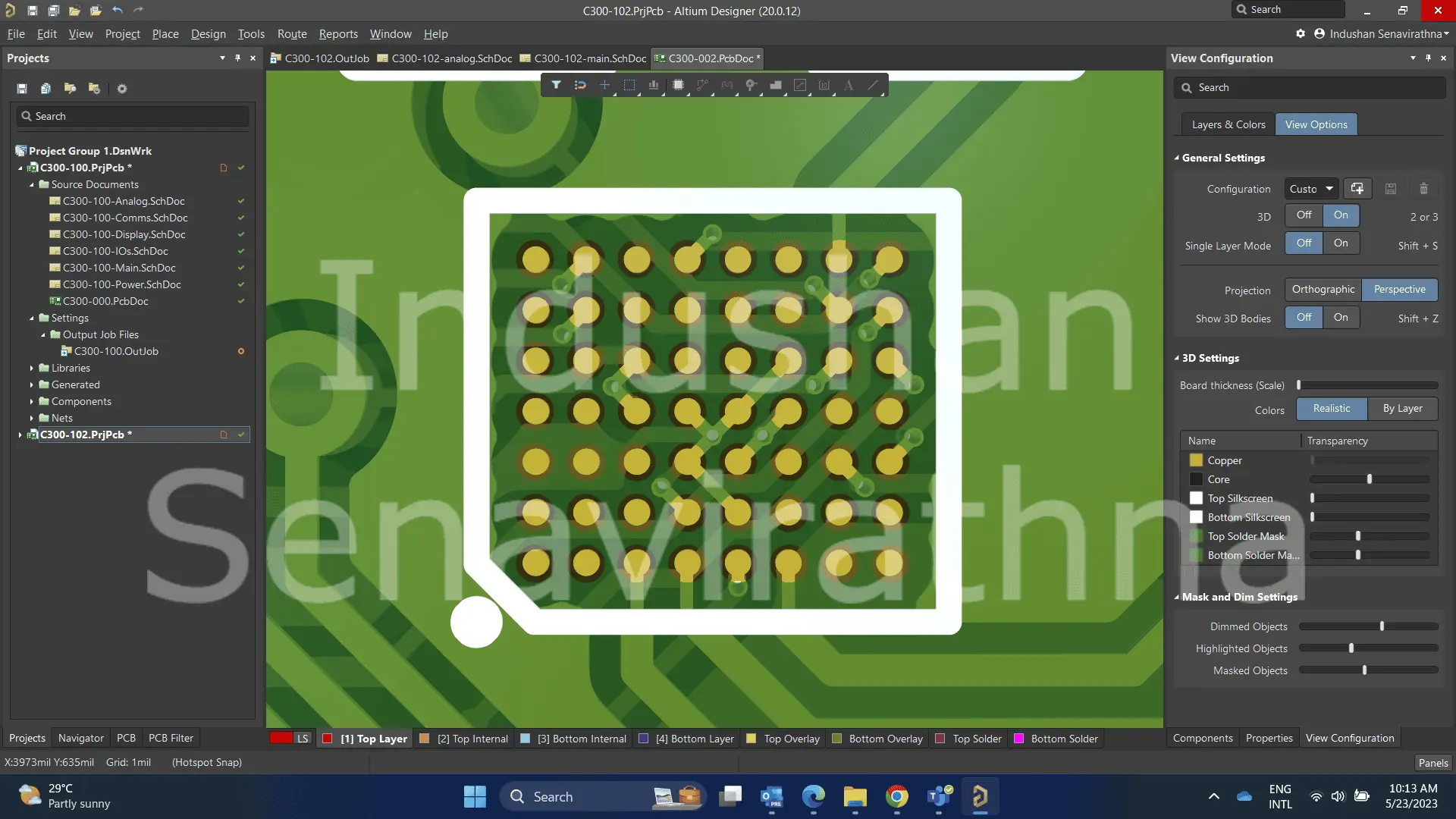
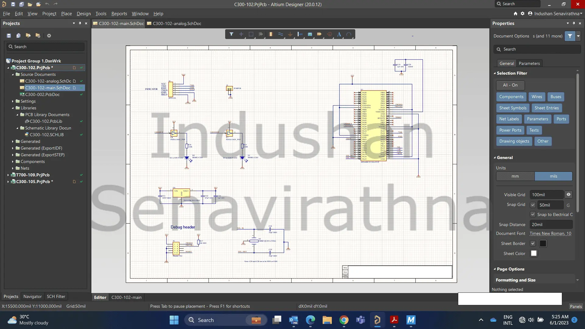
The Analog Accessory Module incorporates a range of carefully selected components to achieve its functionality. The heart of the module is the ATSAMC21J18A – UUT microcontroller, which belongs to the Microchip SAM C21 series of 5V Cortex M0+ devices. Housed in a 56-pin Ball Grid Array (BGA) package with a pad size of 0.2mm, this microcontroller provides the processing power and control necessary for the module's operation.
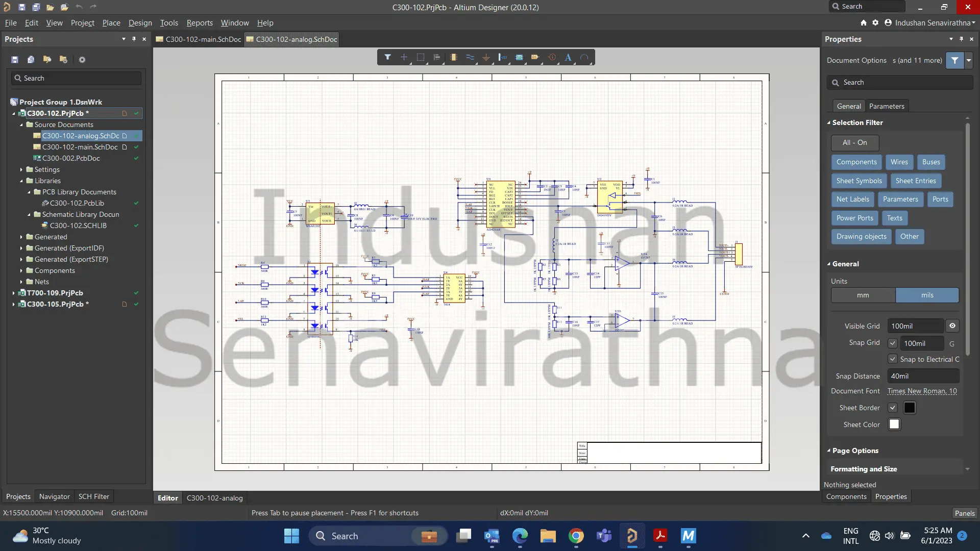
The Digital-to-Analog Converter (DAC) is implemented using the AD420AR, a high-performance and accurate converter. It ensures precise conversion of digital signals to analog outputs, delivering reliable and stable analog signals. To facilitate analog signal routing, the DG419DY analog switch IC is employed. This component offers robust and efficient signal switching capabilities, allowing for seamless control and management of analog signals within the module.
Power conversion within the module is handled by the MASU202 DC-DC converter. This converter efficiently converts power from one voltage level to another, ensuring optimal power utilization and reducing energy loss.
For electrical isolation between different sections of the circuit, the module utilizes the SFH6916 optocoupler. This component provides reliable and secure isolation, protecting sensitive circuitry from potential interference and maintaining signal integrity.
Signal conditioning and level shifting requirements are met using the 7414 Hex Schmitt-Trigger inverter. This component plays a crucial role in adapting and conditioning signals, ensuring compatibility between different parts of the circuit.
The OP297 operational amplifier is employed to provide amplification and signal conditioning capabilities. This component helps in boosting and shaping analog signals, enhancing their accuracy and fidelity.
To ensure a stable and regulated power supply, the module utilizes the TS1117BCW33 RPG voltage regulator. This specific variant of the TS1117 IC delivers consistent and reliable voltage regulation, maintaining the required power levels for various components within the module.
For signal switching and amplification purposes, the module employs PDTA114ET_PNP transistors. These PNP transistors offer excellent switching characteristics and amplification capabilities, enabling precise control and manipulation of analog signals.
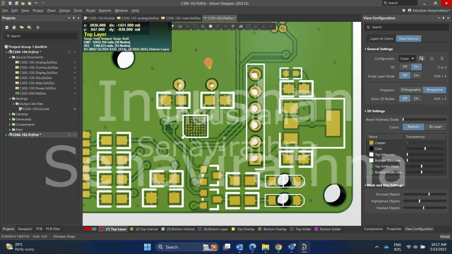
The QC49/A XTAL -2MHZ oscillator component generates a stable 2MHz clock signal. This clock signal is crucial for timing and synchronization purposes within the module, ensuring proper operation and coordination of various components.
analog output, and efficient signal management. The thoughtful combination of these components enhances the module's functionality and enables it to meet the project's requirements effectively.
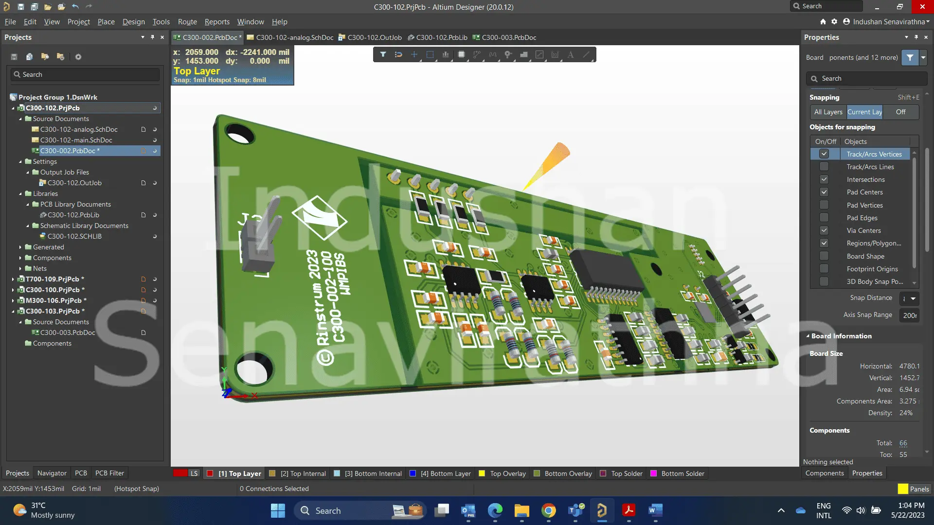
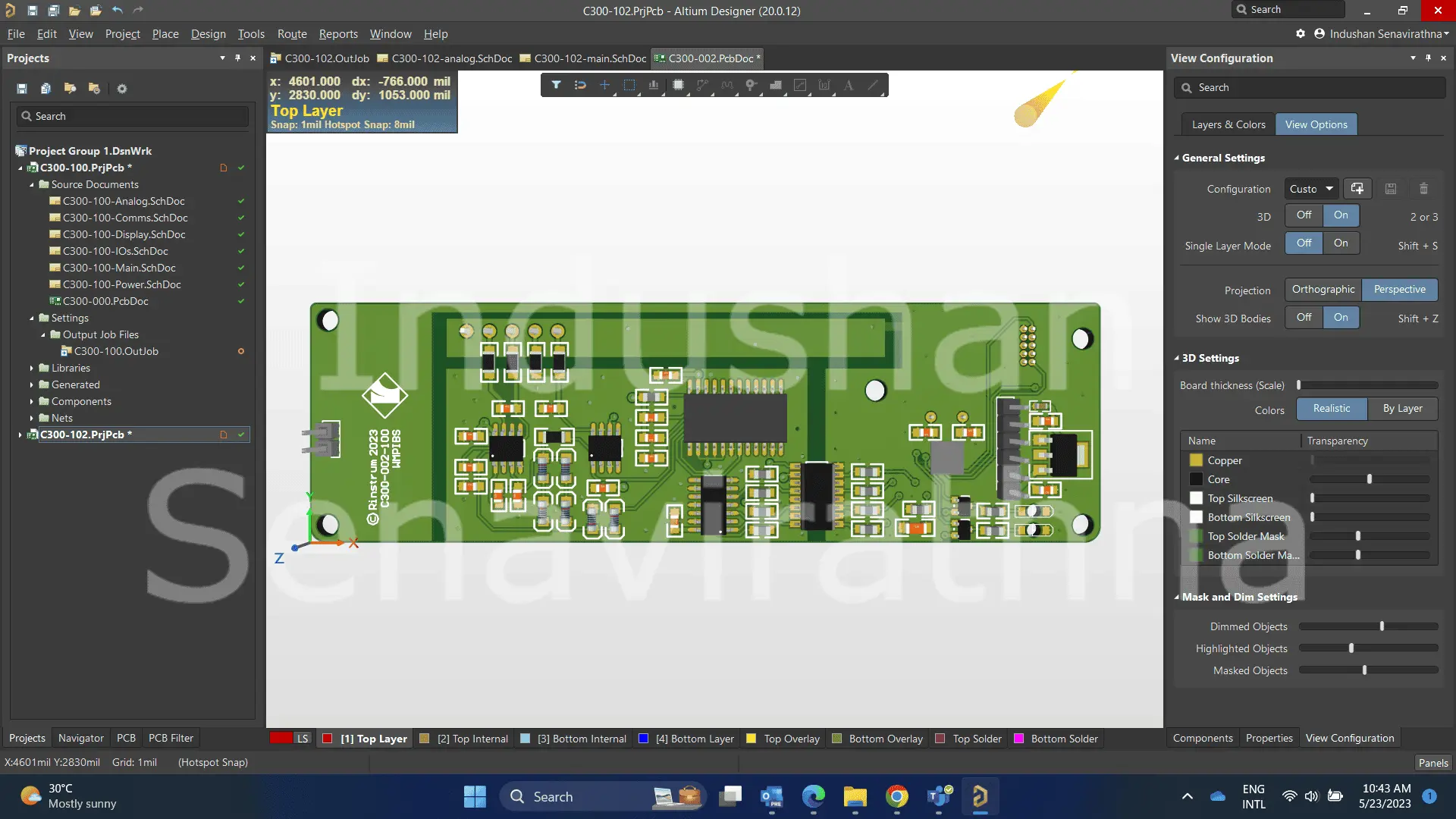
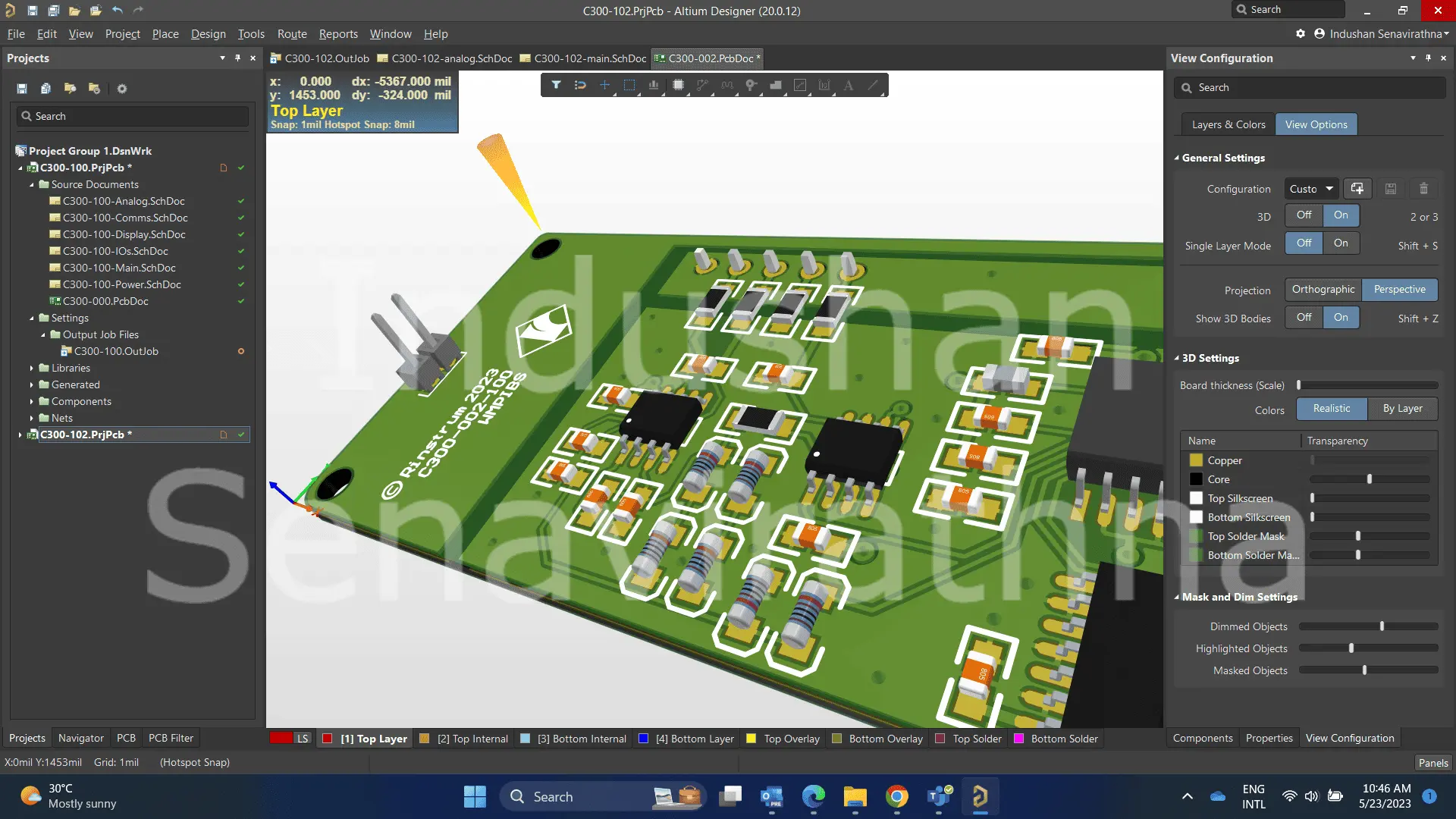
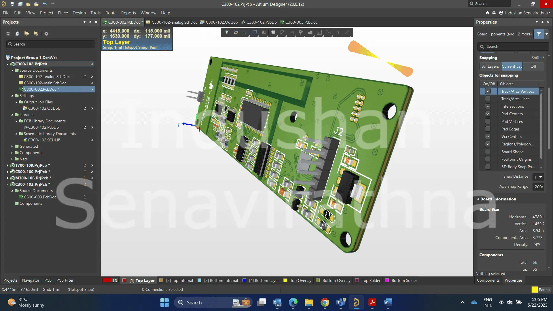
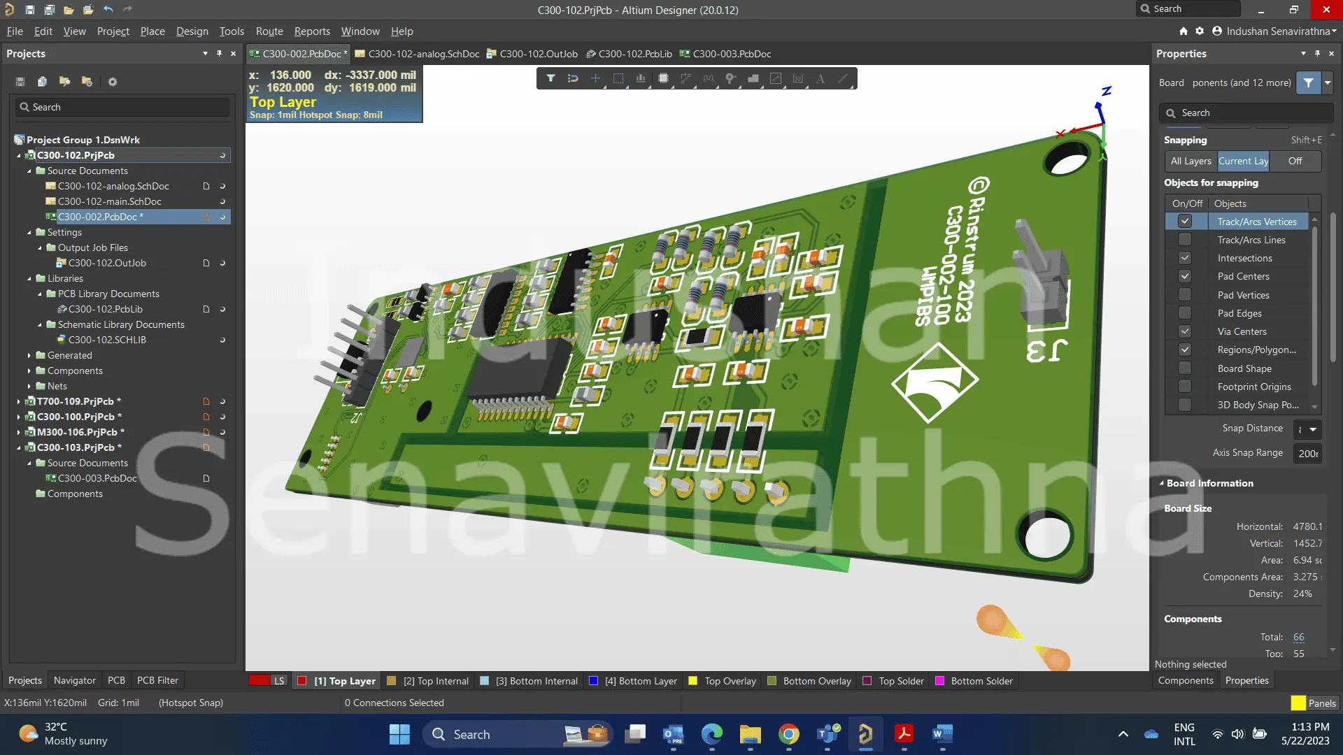
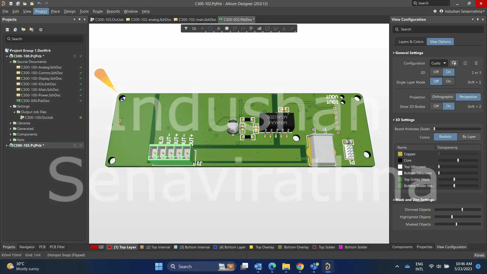
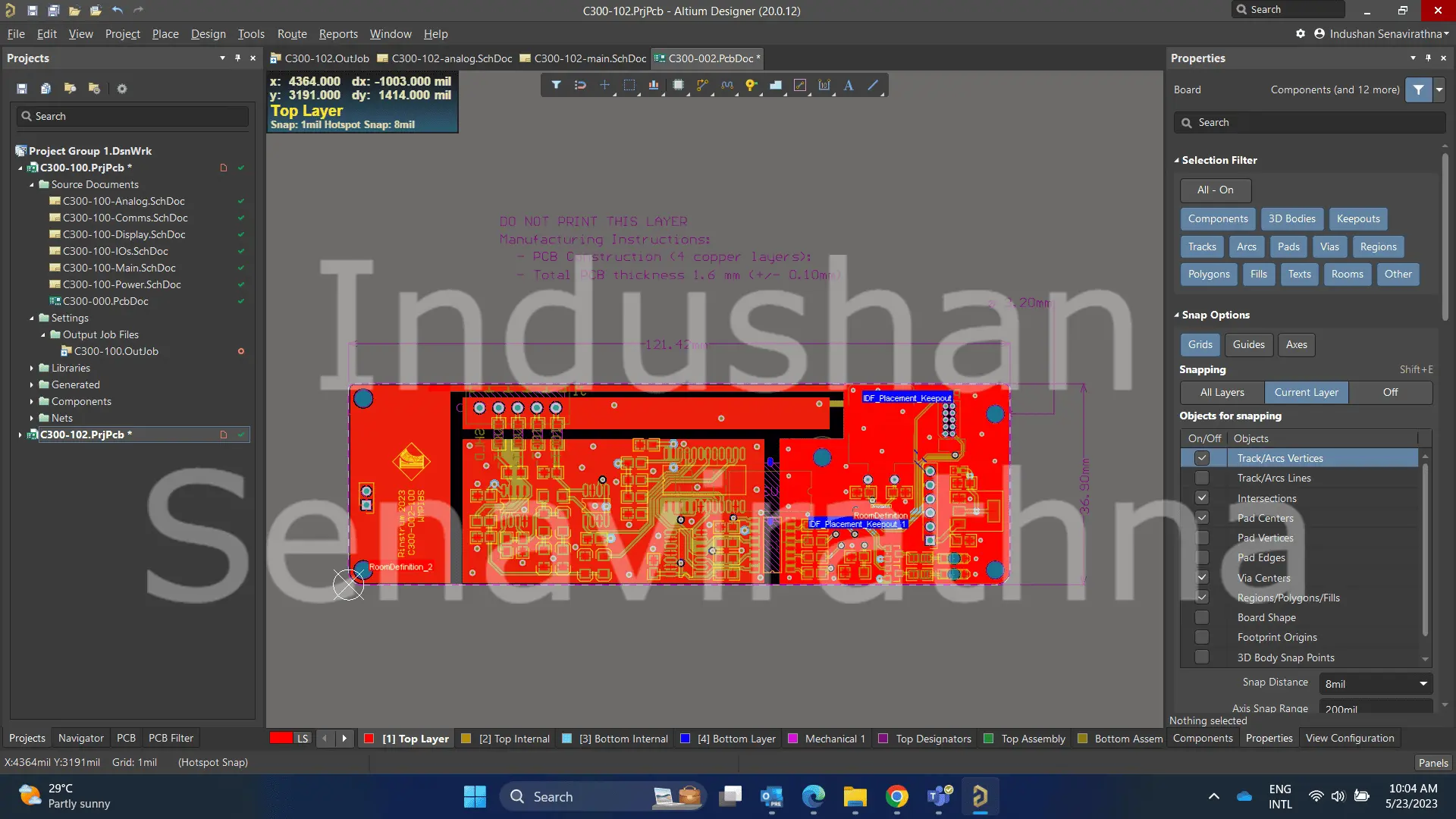
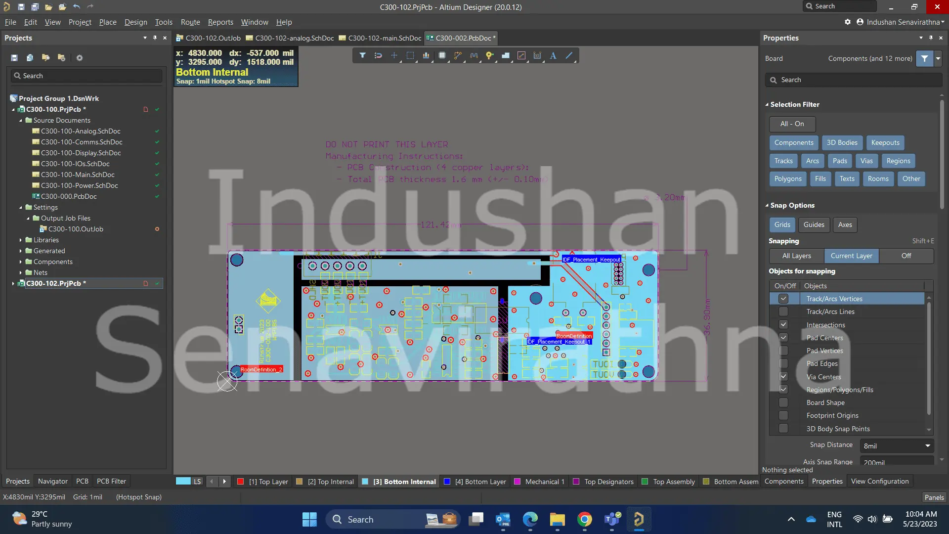
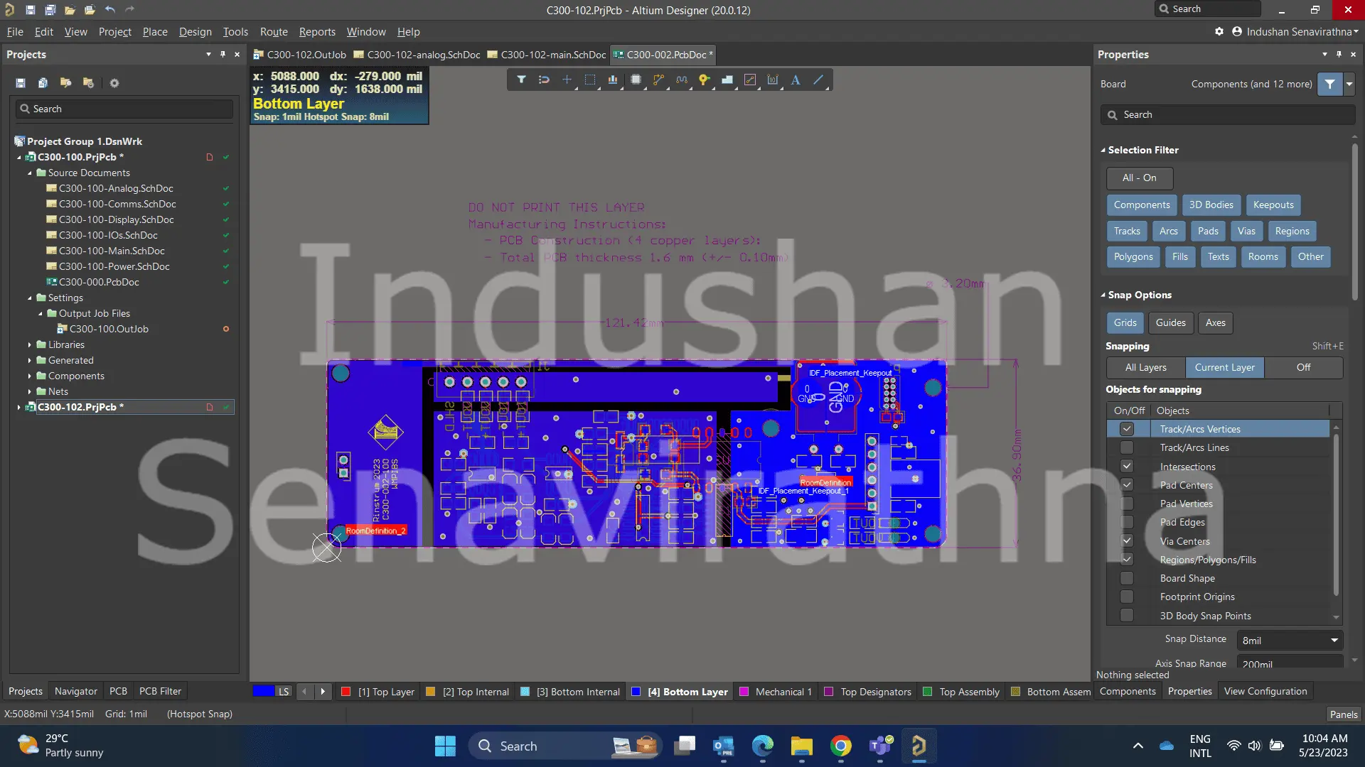
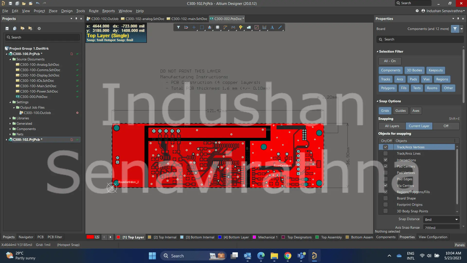
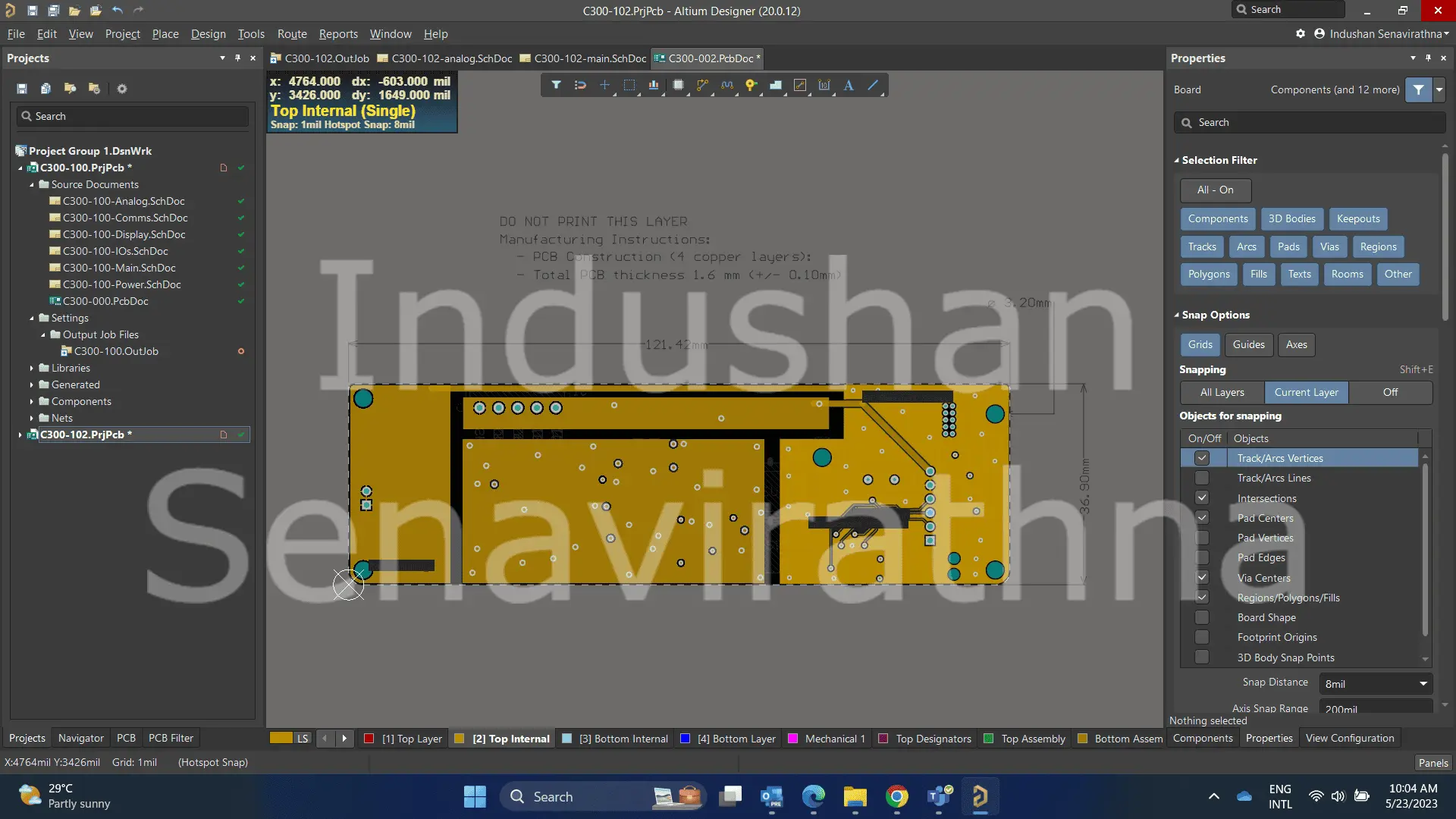
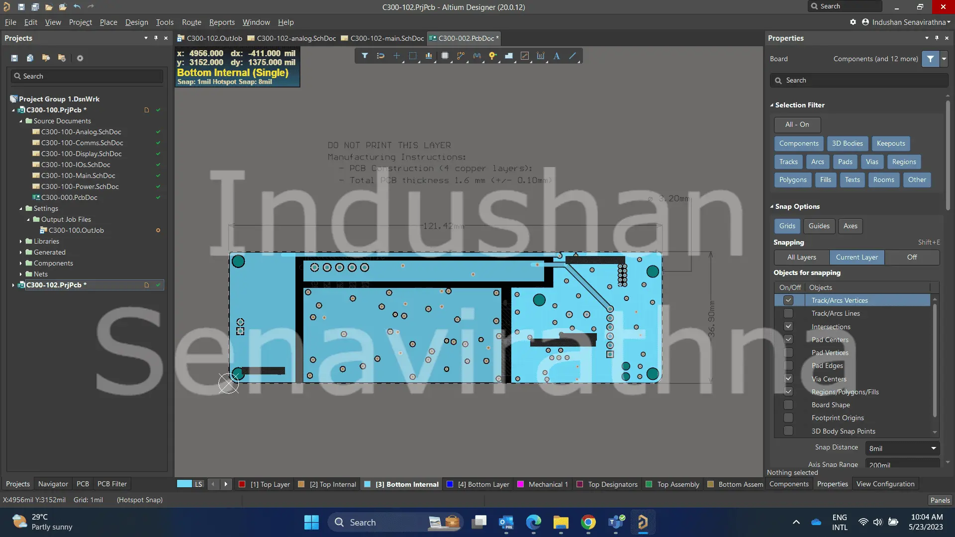
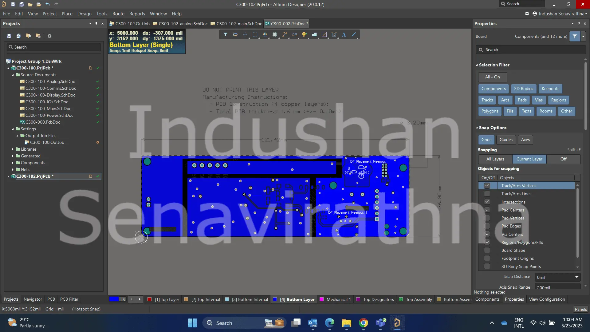
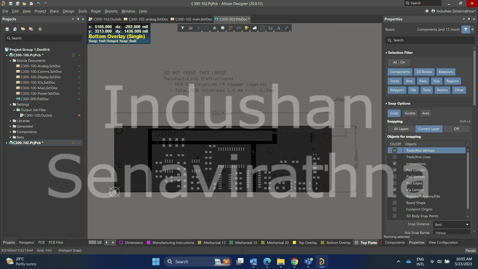
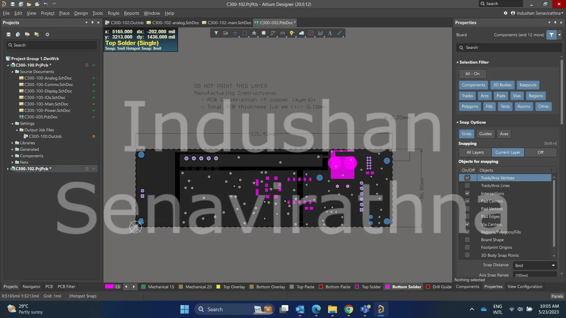
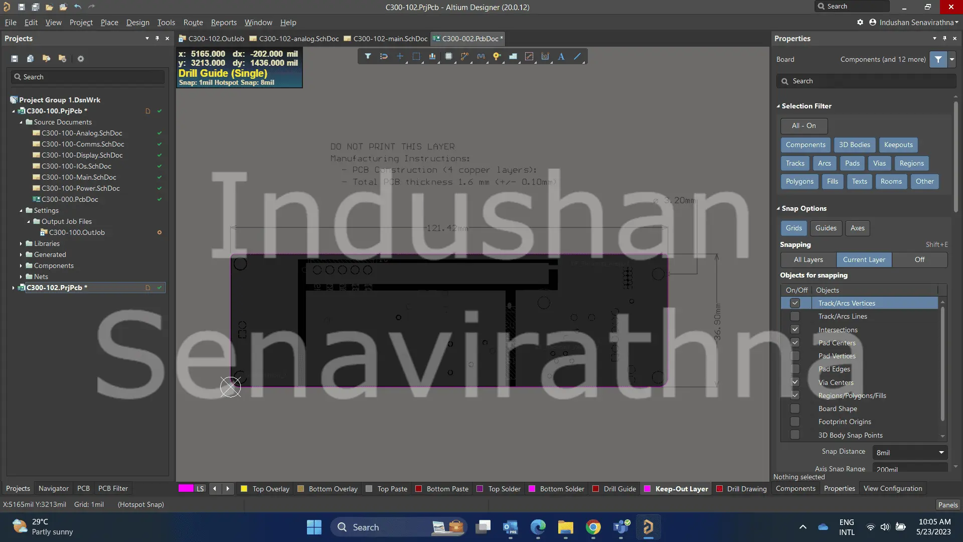
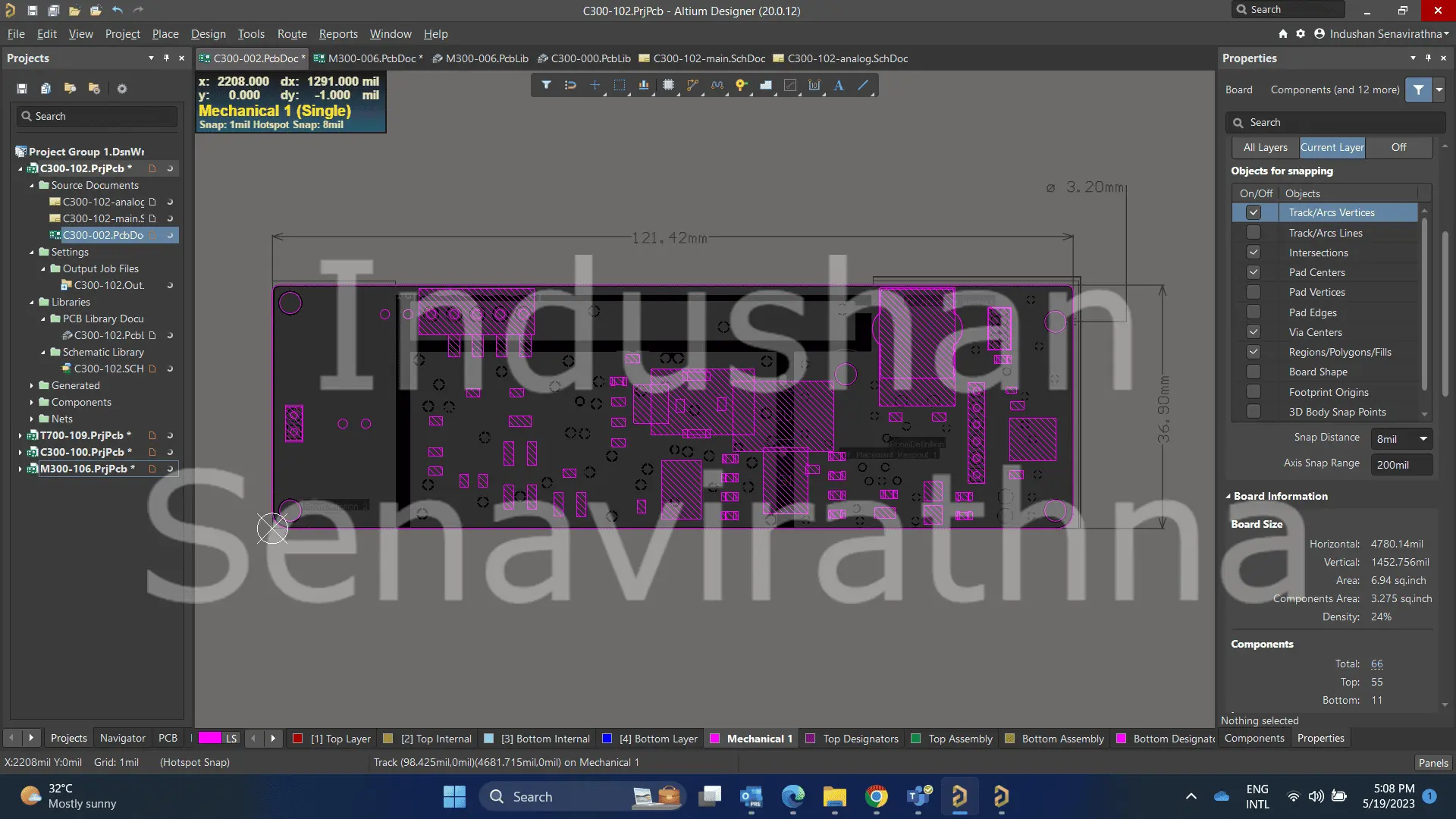
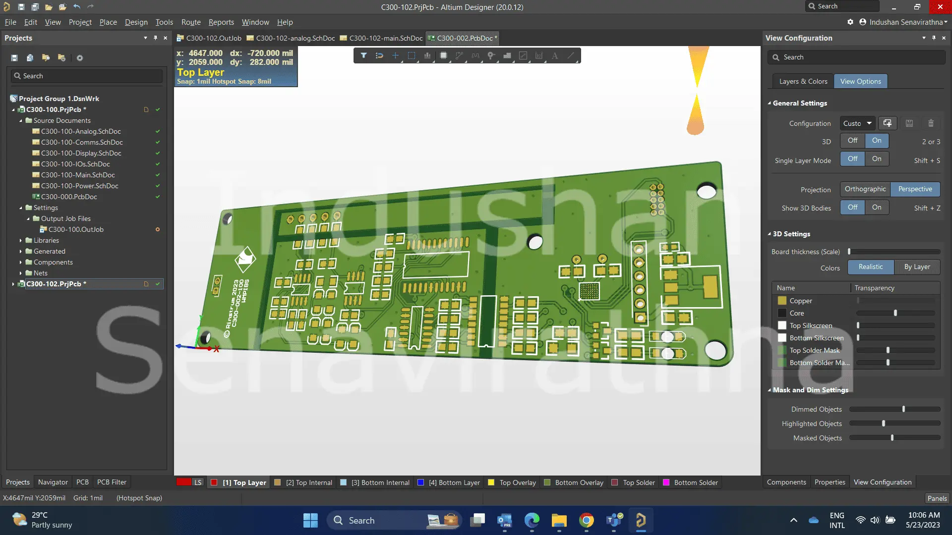
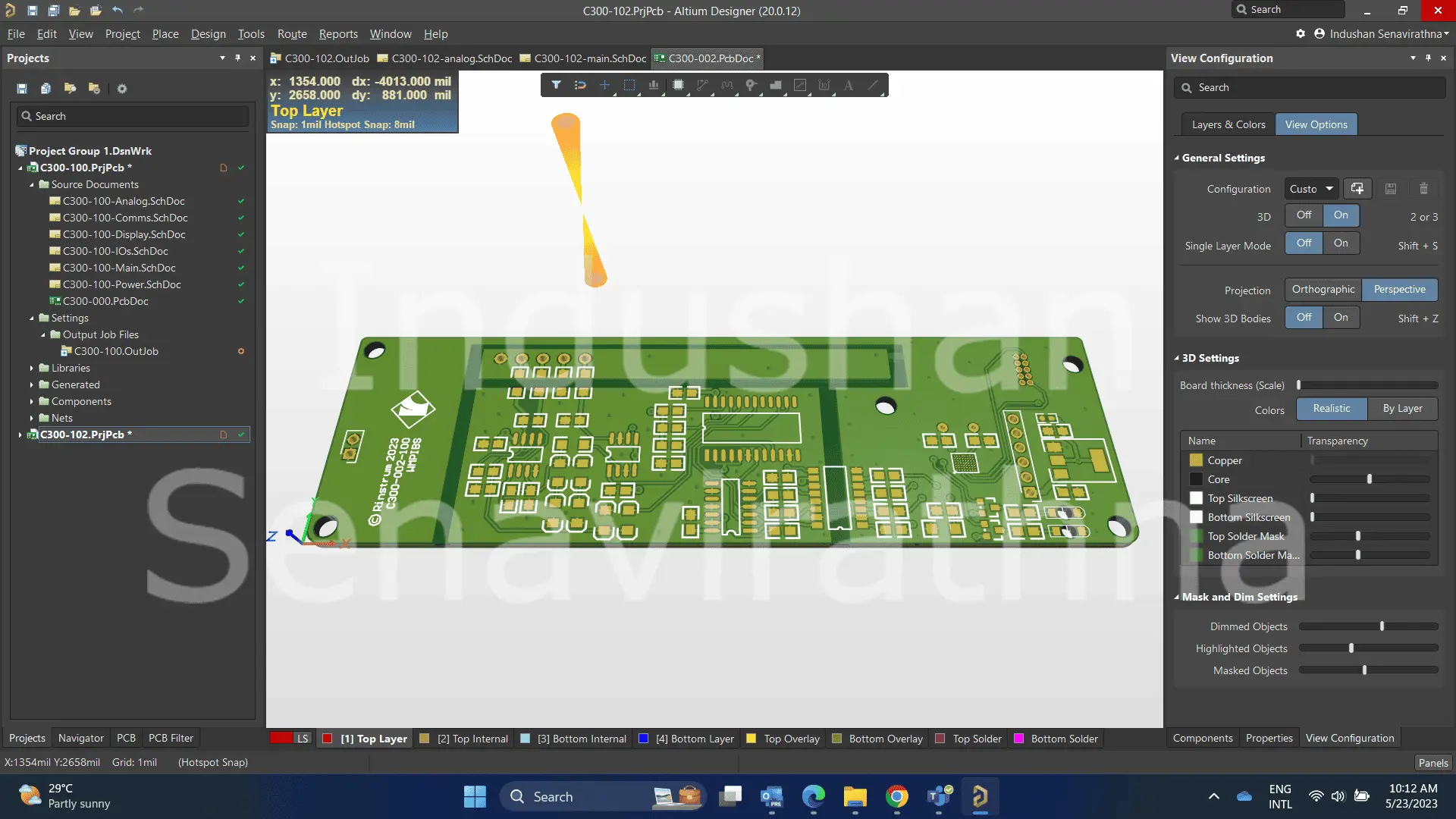
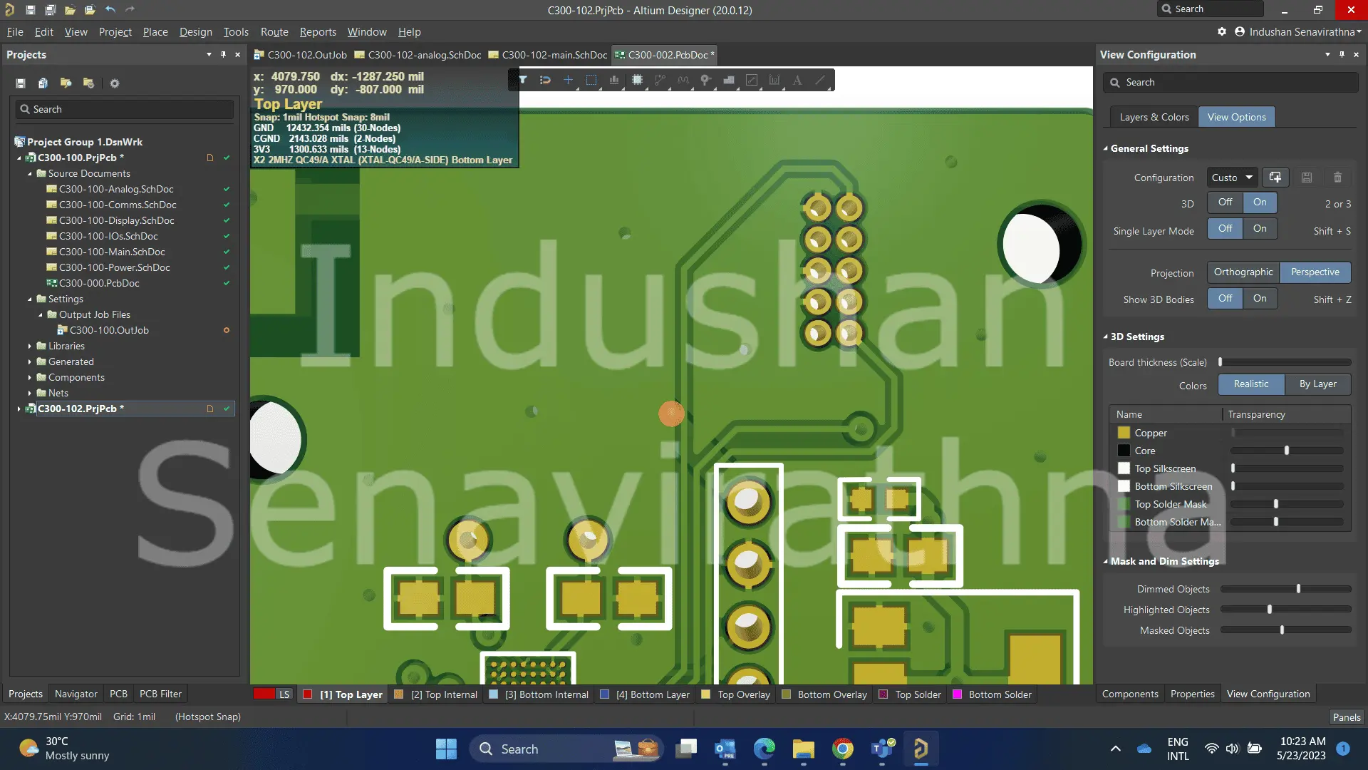
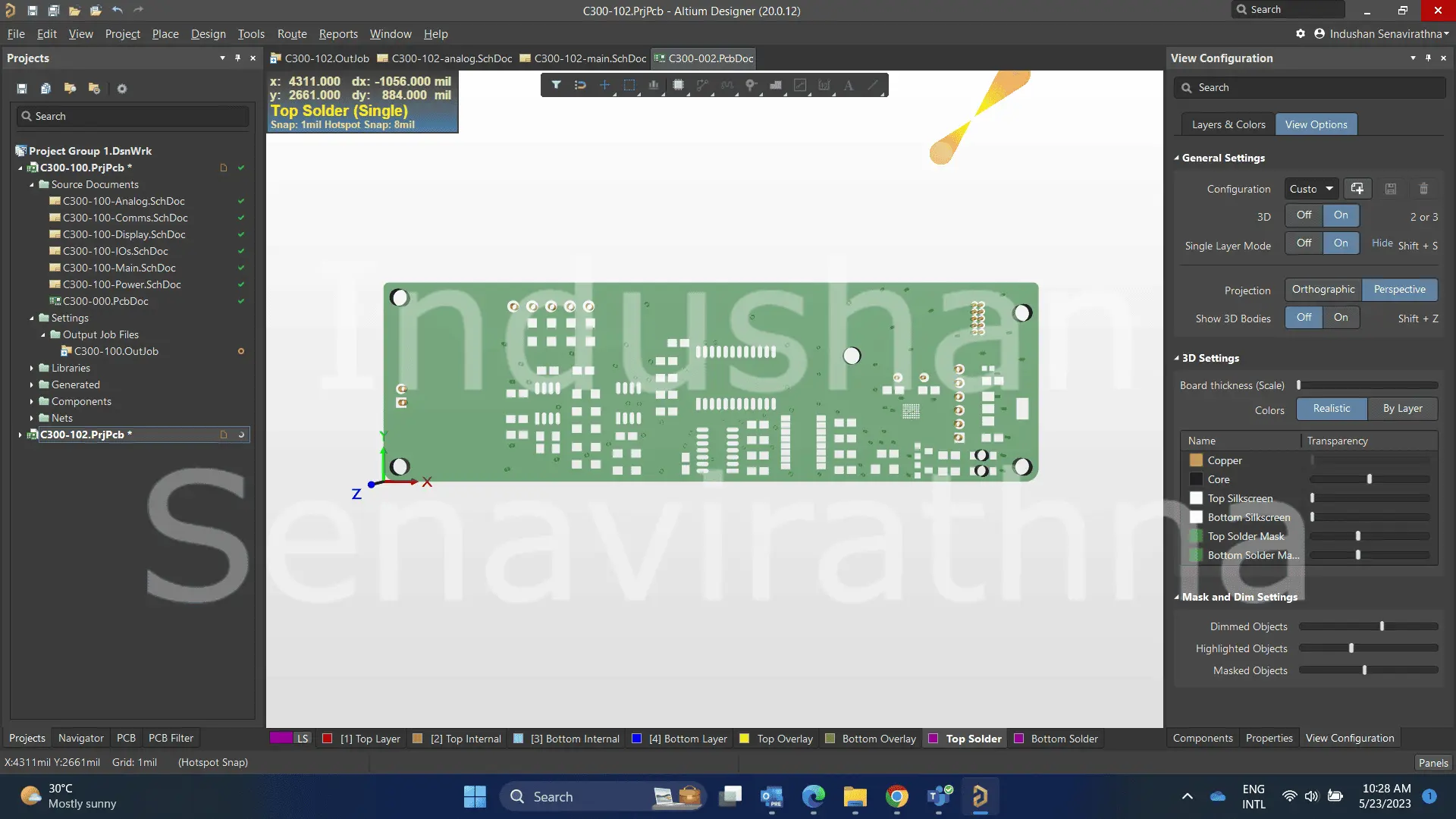
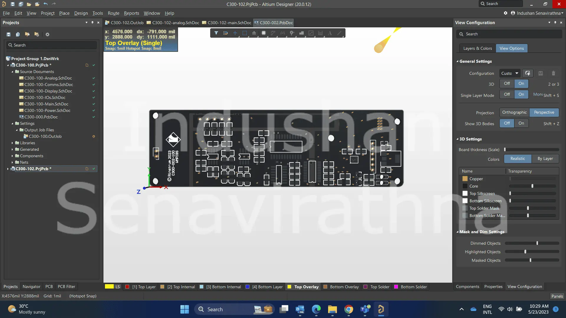
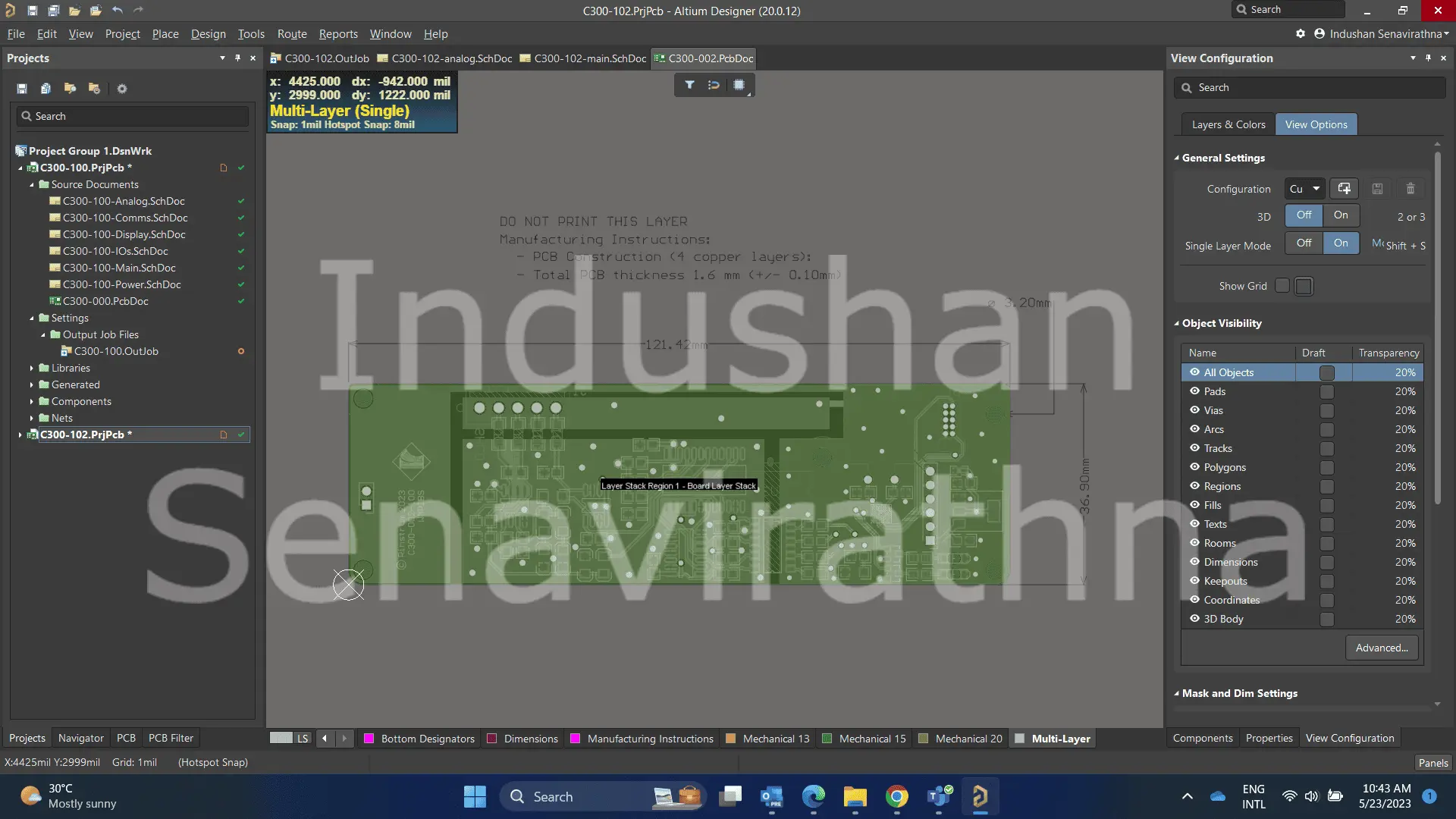
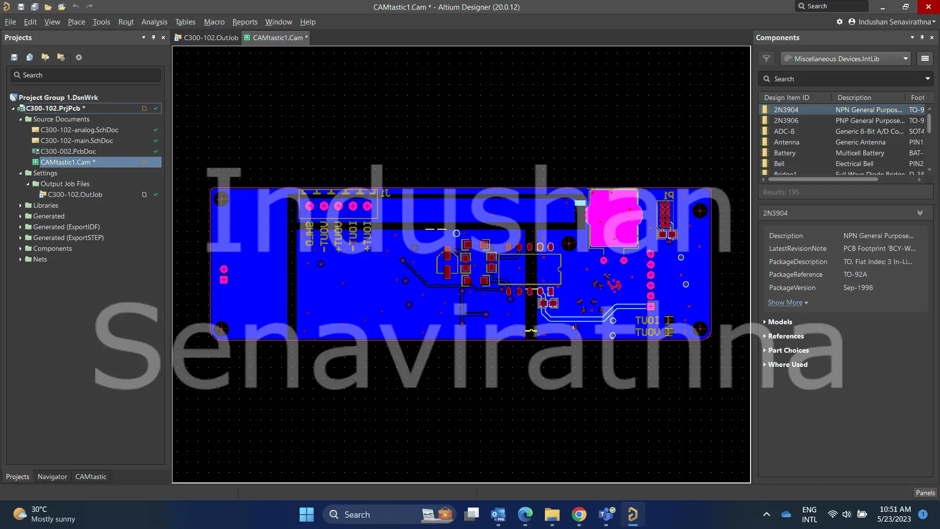
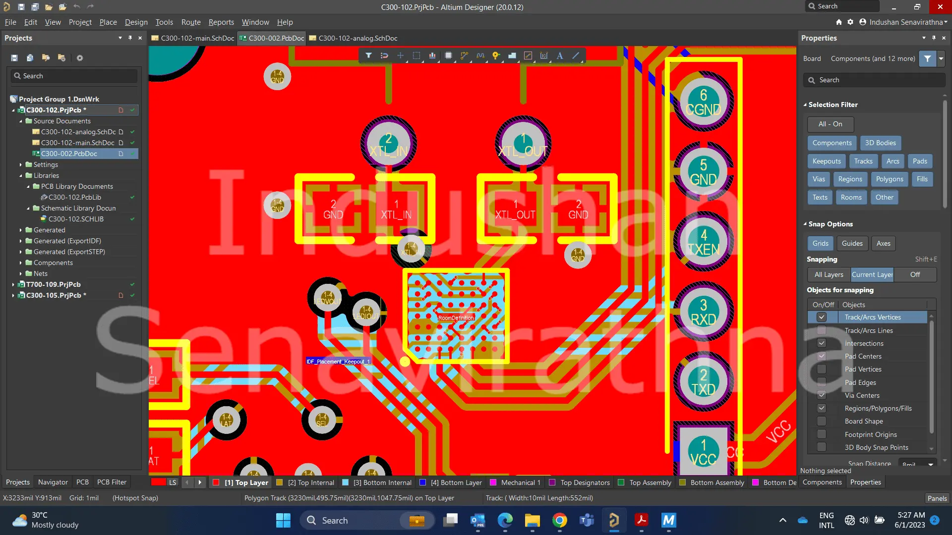
During the development process, I meticulously worked on the block diagram and schematic drawings, creating and verifying component schematic library files. I ensured accurate footprints, proper alignment, and conducted validation to check for any Design Rule Check (DRC) errors. For the PCB layout, I defined layer stacks, added components, and routed the PCB according to IPC regulations. The Microcontroller's BGA Fanout process required special attention due to the small pad size, which necessitated the use of the Doge Bone method. I adhered to international regulations and collaborated with the PCB manufacturer to determine the appropriate vias, considering their capabilities and our requirements.
To meet the highest standards, I meticulously checked each net for any leftover track particles, added polygons, poured, and stitched vias correctly, and performed a comprehensive Design Rule Check. I also implemented specific rules and clearance requirements, particularly for the BGA, by defining separate room definition conditions.
Upon successful completion, I generated the necessary output files, ensuring accurate file names, paths, and documentation. This included schematic documentation, PCB drawing details, layer information, and an Excel and PDF Bill of Materials (BOM).
In conclusion, I have successfully designed a 4-layer PCB for the Analog Accessory Module, showcasing my expertise in analog circuitry, PCB design, adherence to international standards, and effective collaboration with PCB manufacturers.
The main specifications of the Analog Accessory Module are as follows:
- Analog Output: The module provides one isolated analog output with a choice of either 4-20mA or 0-10V signal.
- Isolation: The analog output is isolated with an isolation capability of over 500V from the indicator to the module, ensuring safety and preventing interference.
- Update Rate: The module achieves a high update rate of up to 400Hz, allowing for rapid and accurate analog signal updates.
- Resolution: The module offers a resolution of approximately 1/65,000, equivalent to 16 bits. This high resolution enables precise and fine-grained analog signal representation.
- Current Output Specifications: Analog Rated Load: The module supports a maximum load of 600Ω. Analog Range: The current output range is 0 to 24mA. Analog Error: The overall error for current output is less than 0.1%, ensuring accurate and reliable current signal representation.
- Voltage Output Specifications: Analog Rated Load: The module supports a minimum load of 2000Ω. Analog Range: The voltage output range is -1.5 to 11.5VDC. Analog Error: The overall error for voltage output is less than 0.2%, providing precise and stable voltage signal generation.
Skills
- Schematic Design and Capture
- PCB Layout and Routing
- CAD Software Proficiency (Altium)
- Understanding of Electrical Safety Standards
- Knowledge of Analog Signal Conditioning Techniques
- Familiarity with Microcontroller Programming and Integration
- Testing and Debugging of Analog Circuits
- Troubleshooting and Problem-Solving
- Familiarity with Data Sheet Analysis and Component Datasheet Interpretation
- Collaborative Teamwork and Communication with Colleagues and Stakeholders
- Time Management and Meeting Deadlines
- Knowledge of Industrial Control Systems
- Familiarity with Design for Manufacturing (DFM) Principles
- Understanding of EMI/EMC Considerations in Analog Circuit Design
- Continuous Learning and Adaptability to New Technologies and Industry Trends